
New Delhi: The Central government is gearing up to expand the country’s semiconductor ecosystem under the Semicon 2.0 initiative, targeting the creation of at least 200 chip design startups and companies, alongside training 1 lakh skilled technicians.
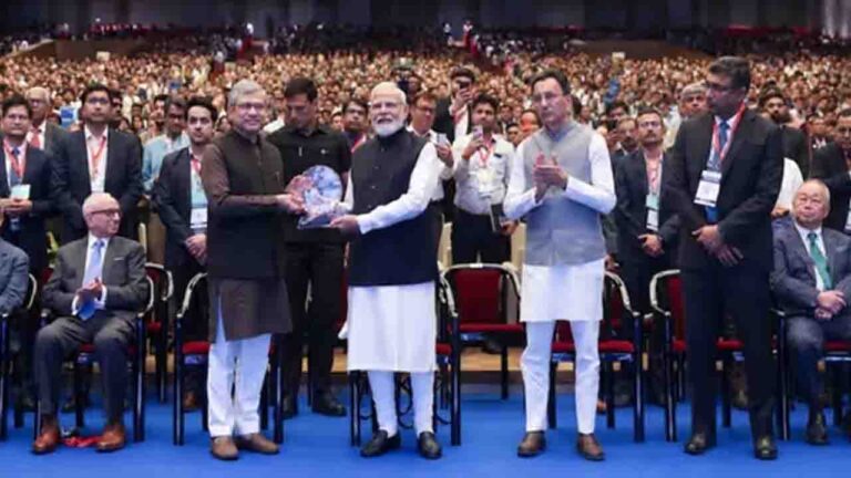
Speaking at the inaugural session of SEMICON India 2026 in New Delhi on September 17, Union Electronics and IT Minister Ashwini Vaishnaw outlined the government’s vision for the next phase. While Semicon 1.0 focused on talent development and building a basic semiconductor ecosystem, Semicon 2.0 will advance chip design, manufacturing, packaging, research, and talent development.
Six Pillars of Semicon 2.0
Chip Design: Serving as the first pillar, the initiative aims to build at least 200 startups and companies focused on chip design for various semiconductor requirements. Under Semicon 1.0, over 105 startups attempted chip design, with around 20 securing venture capital funding totaling nearly ₹800 crore.
Equipment and Materials: The second pillar centers on capital equipment, maintenance facilities, chemicals, and specialized gases.
Fabrication Units: The third pillar focuses on scaling up display, memory, silicon, compound, and logic fabrication units.



Advanced Packaging: The fourth pillar aims to scale advanced packaging, including pushing forward the 3D packaging facility currently coming up in Odisha.
Applied R&D: The fifth pillar prioritizes industry-driven applied research and development by emphasizing collaboration between companies and academic institutions. Vaishnaw urged industry participants to submit project proposals for this initiative.
Talent Development: The sixth pillar targets training 1 lakh skilled technicians, cleanroom personnel, and factory floor workers to supply direct workforce requirements for upcoming semiconductor factories.
Progress and Expansion
Under Semicon 1.0, the government had set a target to train 85,000 design engineers over 10 years. Vaishnaw revealed that 70,000 engineers have already received training within four years. Additionally, over 400 universities have gained access to Electronic Design Automation tools from Cadence, Siemens, and Synopsys, while chips designed by students are undergoing tape-out at the Semiconductor Laboratory in Mohali.
Approved in December 2021 with an outlay of ₹76,000 crore, the initial Semicon 1.0 policy has now evolved into Semicon 2.0, which received approval in July 2026 with a total outlay of ₹1,27,500 crore.